PCB Manufacture
We are specialists in custom PCB manufacturing, both in short series and large productions, with high quality materials and rigorous control
 Skip to content
 We are specialists in custom PCB manufacturing, both in short series and large productions, with high quality materials and rigorous control
At CISA, Circuitos Impresos, S.A., we have been specialists in PCB manufacturing since 1965, positioning us as one of the most experienced and established printed circuit board manufacturers in Spain. We design and produce highly complex printed circuit boards, adapting to the technical needs of each client and project.
We offer solutions in rigid PCBs (from 2 to 20 layers), flexible (up to 10 layers) and Rigid-Flex (up to 14 layers), using certified materials and advanced production processes that guarantee reliability, durability and precision.
We work for demanding sectors such as telecommunications, medicine, automotive, LED lighting, defense, electronics, and consumer goods, always meeting high standards of quality, traceability, and delivery.
Our highly qualified technical team and the use of cutting-edge technology allow us to offer a comprehensive service in the manufacturing of printed circuit boards, from prototype to mass production.
CISA represents trust, innovation and commitment in every PCB we manufacture. We offer the following types of circuits:
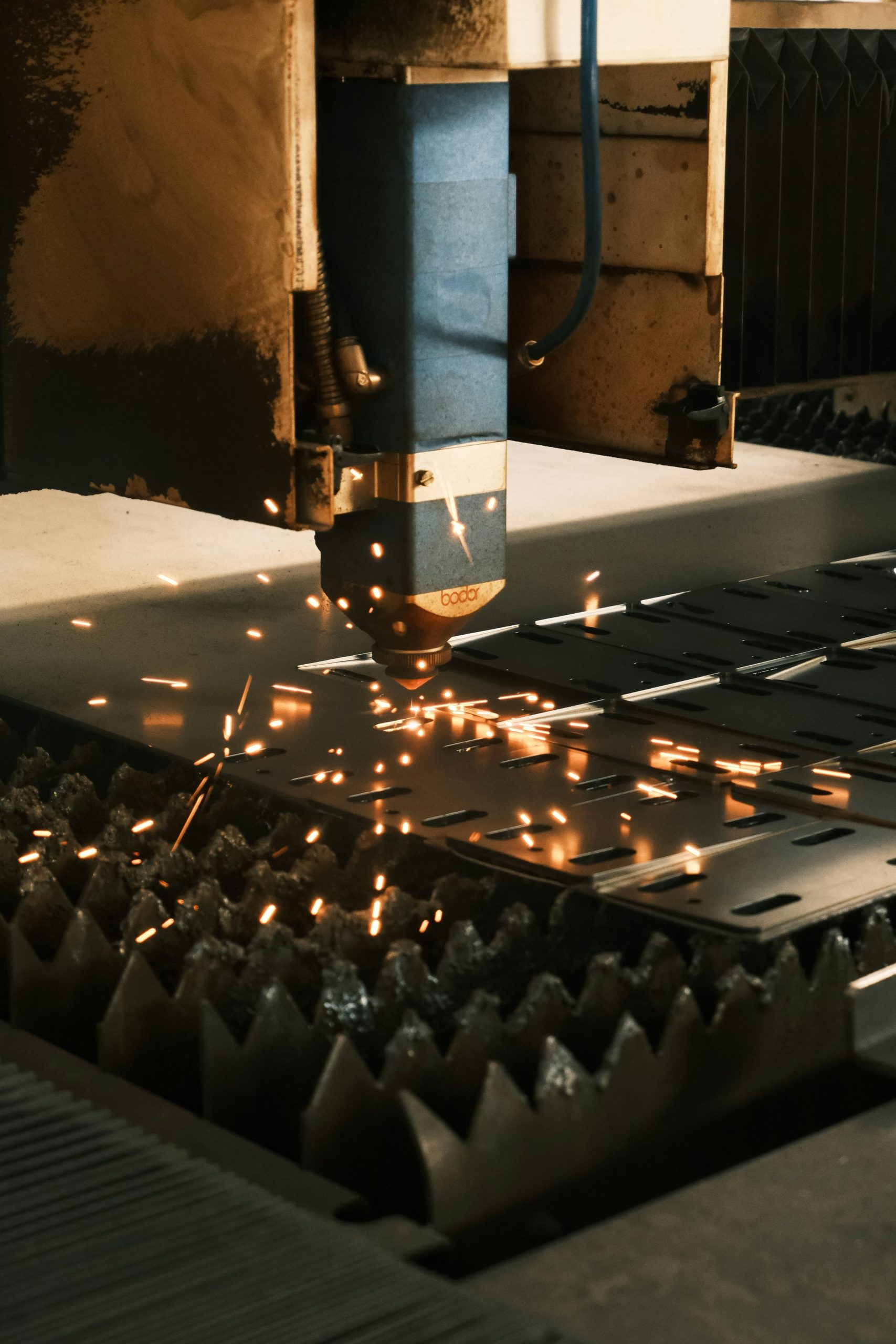
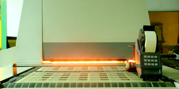
Printed circuit board manufacturing requires precision, reliability, and top-level technology. That's why our plant uses state-of-the-art machinery and automated processes that guarantee high performance at every stage of production.
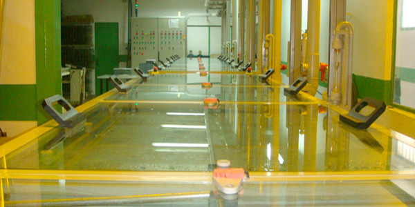
Each section is equipped with fully automated chemical lines, allowing us to maintain a constant and predictable workload, ensuring precise planning and timely delivery of each order.
Our systems are designed to handle everything from short runs to large volumes, always meeting the demanding requirements of sectors such as industry, medicine, aerospace, and telecommunications.
Furthermore, preventive maintenance is essential to ensure the perfect condition of our machinery and avoid unexpected downtime.
We continually invest in upgrading our facilities and adopting the latest printed circuit board technology, ensuring the reliability and quality that each customer expects.
| Base materials | FR4/FR4 HTg/FR2/CEM1/ CEM3/BT-EPOXI/Alta Frecuencia |
| Electrical continuity | Max 10 Ohms |
| Aspect Ratio | 1:14 |
| Ionic contamination | Max 1micrEquivgr NaCl/cm2 |
| Impedance control | Yes |
| Fire rating | 94V-0 (MOT 105º,130º) |
| Finishes | Rohs, non-Rohs |
| Gold edge connectors | Yes |
| Graphite connectors | Yes |
| Kapton/peelable tape | Yes |
| Component marking: | Yes |
| Polymerised drills | Yes |
| SURFACE GEOMETRY (X and Y axes) | |
| Max. dimensions | 600×600 mm |
| Width/Space of/between conductors | 0.10 mm |
| Min. diameter | |
| Plated drills | 0.2 mm |
| Non-plated drills | 0.3 mm |
| Buried drills | 0.2 mm |
| Microvia | 0.1 mm |
| Registration accuracy | |
| External drills/pads | max 0.1 mm |
| Internal drills/pads | max 0.15 mm |
| Drill/contour | max 0.1 mm |
| Pad/soldermask | max 0.1 mm |
| Between layers | max 0.1 mm |
| Drill diameter tolerance | |
| Plated | -0.0/+0.1 mm |
| Non-Plated | -0.0/+0.05 mm |
| Exterior profile tolerance | ± 0.1 mm |
| Non-plated space for grooving | min 0.8 mm |
| Groove position error | ± 0.10 mm |
| Photosensitive ink trace width | min 0.12 mm |
| Distance between copper pad/photosensitive ink | min 0.12 mm |
| Legend trace width | min 0.12 mm |
| Graphite trace width | min 0.5 mm |
| Space between graphites | min 0.4 mm |
| Space between graphite/copper | min 0.4 mm |
| Peelable margin | min 0.4 mm |
| Space between peelable/node | min 1.0 mm |
| Max. diameter peelable mask drills | 1.8 mm |
| MICROSECTION (Z axis) | |
| Number of layers | 1-12 |
| Base material thickness | 0.5/0.8/1.0/1.2/1.6/2.0/2.4/3.2 |
| Plating thicknesses | |
| Conductors (min Cu) | 25 μ |
| Drill (min Cu) | 25 μ |
| Buried drills (min CU) | 15 μ |
| Overhang | min 15 μ |
| Grooved bore (tolerance) | ± 0.1 mm |
| Bow and twist | Max 1% |
| Chamfer G/F angle | 20º,30º,45º |
Our technical teamis led by chemical science graduates and with a wealth of experience garnered over years spent studying printed circuit processes, who are ideally placed to provide solutions to any problems relating to the manufacture of PCBs.
The chemical laboratory is equipped with everything necessary for appropriate analysis and testing during each chemical process:
Countless other standards and protocols to obtain 100% quality control and assurance during the manufacturing process.


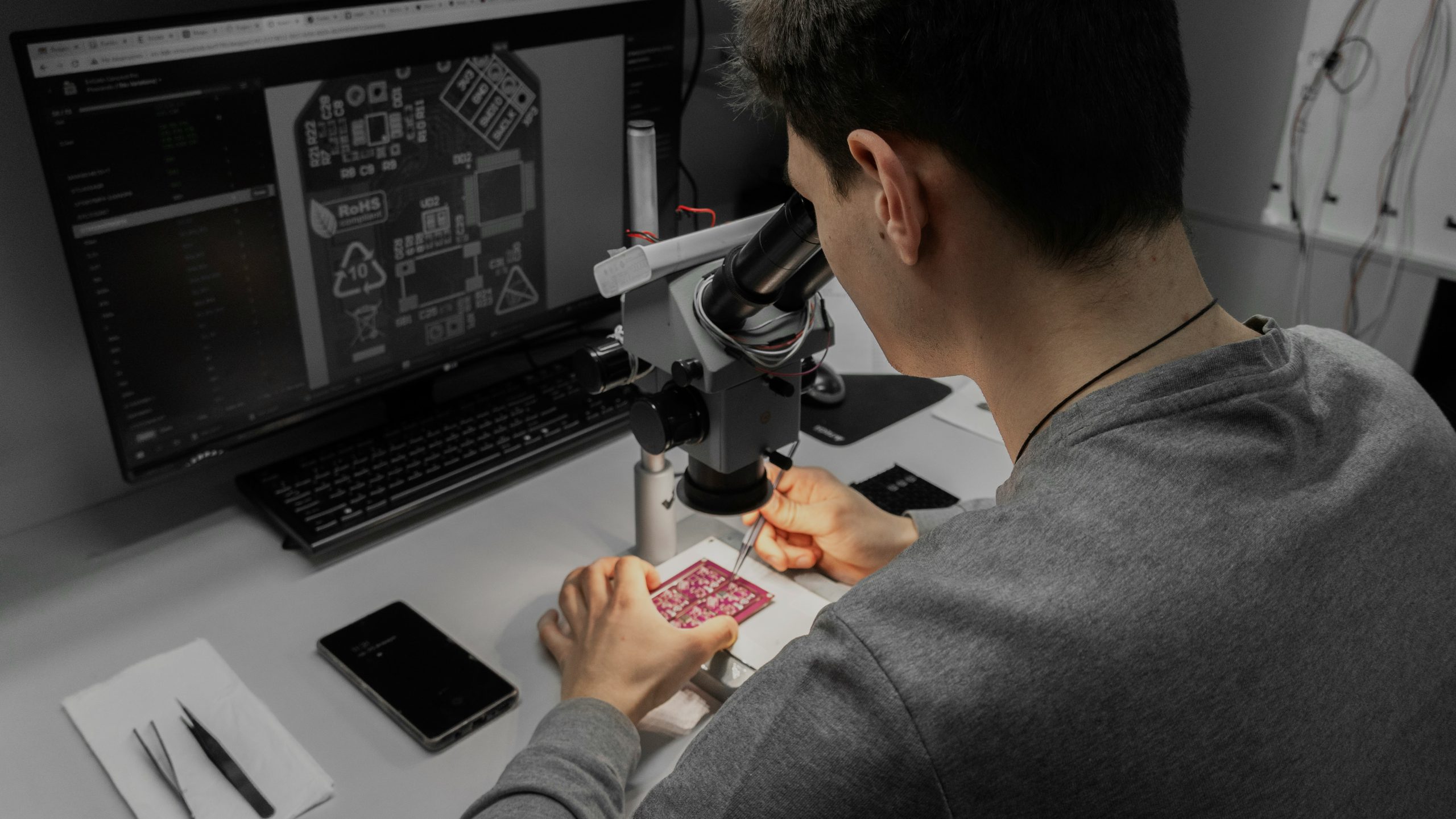
Our Engineering Department is comprised of highly qualified professionals who are continuously trained in the latest technologies applied to the design and manufacturing of printed circuit boards. This training allows us to develop products with optimized designs, perfectly tailored to each client's specifications, and with reliable results from the first unit.
Each new project received is subject to a detailed technical protocol that classifies the documentation by type and generates a specific Worksheet. It defines all the steps and quality controls, both general and specific, that will be applied during circuit manufacturing.
We have a team specialized in processes, time, and materials, responsible for optimizing every phase of production. This precise resource management allows us to rigorously plan our workload and meet our agreed-upon delivery deadlines.
To ensure maximum efficiency and control, we have CAD systems for master generation, CNC programming for drilling, integrated databases for optical and electrical testing, and automatic electrolytic lines. All of this is geared toward a single objective: offering printed circuit board manufacturing with the highest quality standards.
We have a highly qualified team and a solid track record dating back to 1965, which allows us to offer comprehensive and customized solutions in the printed circuit board (PCB) sector. Our priority is to ensure the success of each project, adapting to technological advances and market demands.
We transform your idea into a functional printed circuit board, managing every phase of the process with precision: from the initial concept to the final product.

Lorem ipsum dolor sit amet, consectetur adipiscing elit. Ut elit tellus, luctus nec